

Material: | FR4 | Layer: | 4L |
Board thickness: | 2.0mm | Min Hole: | 0.2MM |
Copper thickness: | 2OZ | Solder mask: | Green |
Min Width & Space: | 6mil/6mil | Silkscreen: | White |
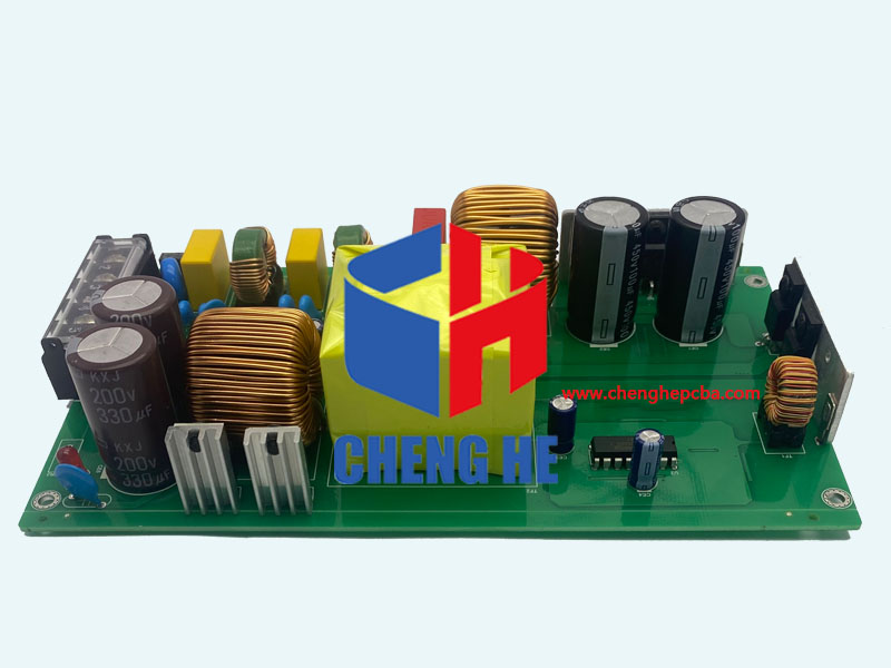
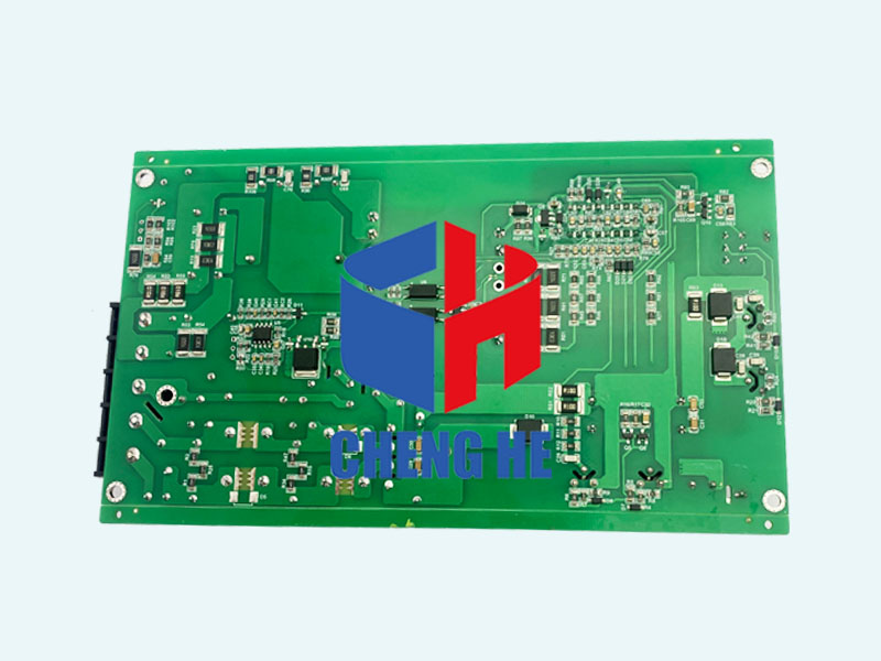
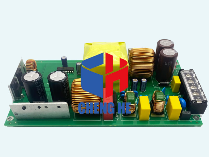
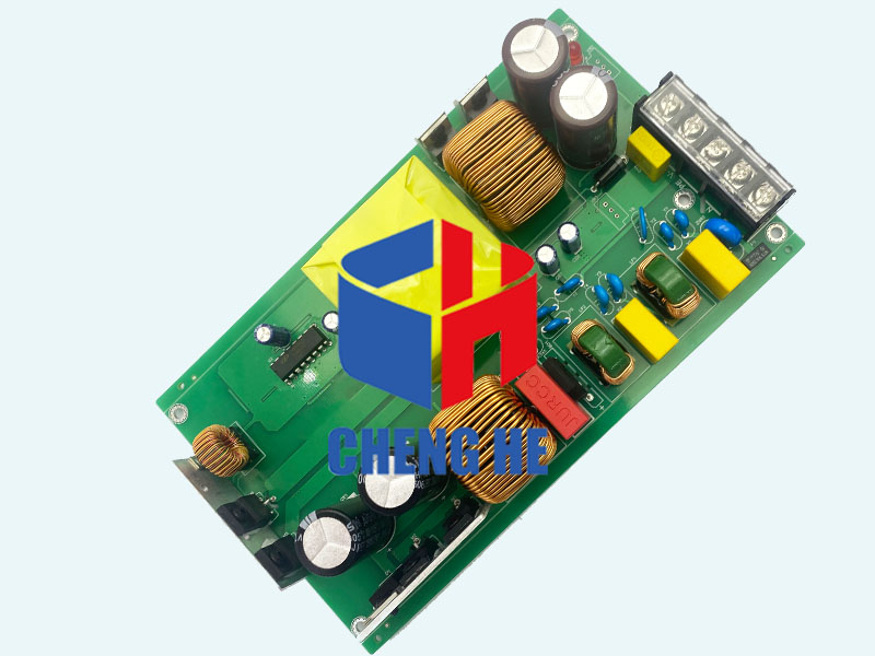
Finishing: | HAL LF | Application: | Power supply PCBA |
PCB assembly: | Wave soldering | Min Component: | 0603 |
How to optimize the heat dissipation performance of power PCB?
The following are the core strategies for optimizing the heat dissipation performance of power PCB, and the comprehensive multi-dimensional technical solutions realize efficient thermal management:
1. PCB structure optimization design
Multilayer board stacking optimization
When using a stacking structure of four layers or more, the complete ground plane is used as the middle layer, and a thermal via array (spacing 1-2mm) is arranged under the heating device, which can reduce the local temperature by 5-8℃.
Copper foil reinforcement strategy
The power area uses 2oz or more thick copper foil, and solid copper is used instead of grid copper. At least 100mm² copper foil area is configured for each watt of power consumption. For example, a 5W device requires a 500mm² copper cladding area.
2. Application of key heat dissipation technologies
Thermal via array technology
Set a via array with a diameter of 0.3mm under heating components such as MOS tubes and inductors, and fill it with thermal conductive silver paste to improve the heat dissipation efficiency by 30%.
IC back copper exposure treatment
By removing the solder mask on the back of the heat-generating chip and directly exposing the copper layer, the thermal resistance between the copper skin and the air can be reduced, and the natural convection effect can be enhanced.
Embedded heat dissipation components
High-end scenarios can use embedded copper blocks or board edge heat dissipation teeth design, which can reduce the local temperature by 15℃ and increase the heat dissipation area by 20%.
3. Layout and process enhancement
Heat source partition layout
Distribute the heat-generating components close to the edge of the PCB, optimize the spacing ≥3mm, and avoid the proximity of temperature-sensitive components such as electrolytic capacitors to power devices.
Layered routing optimization
High current paths are preferentially arranged in the outer layer, and the inner layer routing needs to increase the width by 20% to compensate for the heat dissipation disadvantage. 10A current requires 7mm wide 1oz copper foil routing to control the temperature rise of 10℃.
Surface treatment process
Key solder joints are treated with immersion gold to improve the heat radiation efficiency, and high current contacts are riveted with copper pillars to enhance mechanical and thermal conductivity.
4. Innovation of heat dissipation materials
Substrate upgrade solution
Aluminum or copper substrates are used in high power density scenarios, and the thermal conductivity is 5-10 times higher than that of FR-4. Ceramic substrates can be introduced in extreme environments.
Liquid metal thermal conductivity system
The liquid metal circulation heat dissipation structure driven by an electromagnetic pump is used, combined with micro heat dissipation fins, which is suitable for compact and high-precision equipment.
5. Verification and test standards
Thermal simulation double insurance
ANSYS Icepak simulation is used in the design phase, focusing on the heat island effect in the area with dense vias, and the measured error must be controlled within 3°C.
Aging test specification
Conduct a 72-hour continuous load test at an ambient temperature of 85°C to ensure that the junction temperature of the device is lower than 80% of the specification value.
Through the above comprehensive solution, the heat dissipation efficiency of power PCBs can be increased by more than 40%, meeting the stringent requirements of industrial-grade equipment for temperature rise control and long-term reliability.


 whatsapp